|
EN
|
|
|||||||||||||||
|
WHOLESALE DISTRIBUTOR OF COMPUTER HARDWARE AND CONSUMER ELECTRONICS
|
||||||||||||||||
|
||||||||||||||||
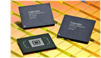
Toshiba to Launch Worlds First 32nm Process NAND Flash Memory Toshiba Corporation, reinforcing its leadership in the development and fabrication of cutting-edge, high density NAND flash memory, has announced that it will start shipping NAND flash memory products fabricated with 32nm process technology. Toshiba Corporation, reinforcing its leadership in the development and fabrication of cutting-edge, high density NAND flash memory, has announced that it will start shipping NAND flash memory products fabricated with 32nm process technology. Samples of the worlds first 32nm generation, 32-gigabit (Gb) single chips (4 gigabytes (GB)), offering the largest density of any NAND flash chip, are available from today, and 16Gb chip (2GB) products, the current mainstream density, will be available in July in Japan. The 32Gb chips will first be applied to memory cards and USB memories and subsequently extended to embedded products. Toshiba is leading the industry in applying 43nm process technology to 32GB products, which stack eight 32Gb NAND flash memory chips. Application of the advanced 32nm process technology will further shrink chip size, allowing Toshiba to boost productivity and bring further enhancements to high density, small sized products. As more mobile phones and mobile equipment provide support for video and movies, demand for larger density, small sized memory products is growing stronger. By leading the industry in transition to finer geometry, Toshiba aims to reinforce and extend its leadership in the NAND flash memory market. Toshiba will start mass production of 32Gb NAND flash memories in July 2009, two months ahead of its original plan. 16Gb products will start to ship from the third quarter of FY2009 (October to December 2009). The new chips will be produced at Toshibas Yokkaichi Operations, in Mie prefecture, Japan. By accelerating process migration and integrating multi level cell technologies, and through continued advances in productivity, Toshiba intends to enhance its competitiveness in the memory business. Source: Toshiba Corporation |