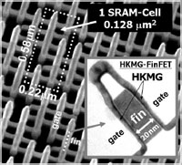
Toshiba Corporation, IBM and AMD has announced that they have together developed a Static Random Access Memory (SRAM) cell that has an area of only 0.128 square micrometers (μm2), the worlds smallest functional SRAM cell that makes use of fin-shaped Field Effect Transistors (FinFETs).
The cell, developed with a high-k/metal gate (HKMG) material, offers advantages over planar-FET cells for future technology generations. SRAM cells are circuit components in most systems-level, large-scale integrated circuits such as microprocessors, and smaller SRAM cells can help provide smaller, faster processors that consume less power.
To reduce the transistor size when SRAM cells are created using conventional planar transistors, IC manufacturers generally adjust properties by doping more impurities into the device area. However, this adjustment creates undesirable variability and deteriorates the SRAM stability. This issue is becoming critical, especially at the 22nm technology node and beyond. The use of FinFETs -- vertical transistors with fin-shaped undoped silicon channels -- is an alternative approach to allow SRAM cell size reduction with less characteristic variation.
Researchers from the three companies fabricated a highly scaled FinFET SRAM cell using HKMG. It is the smallest nonplanar-FET SRAM cell yet achieved: at 0.128μm2, the integrated cell is more than 50 percent smaller than the 0.274μm2 nonplanar-FET cell previously reported. To achieve this goal, the team optimized the processes, especially for depositing and removing materials, including HKMG from vertical surfaces of the non-planar FinFET structure.
By successfully fabricating highly scaled FinFET SRAM cells with HKMG, the companies have positioned FinFETs as an attractive transistor structure for SRAMs in the 22nm node and beyond. The new technology is a step forward to more powerful practical devices.
Источник:
Toshiba