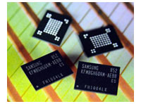
Samsung Electronics has recently announced that it has begun using 40nm process technology to produce an 8Gb Flex-OneNAND fusion memory chip, which supports both single-level cell (SLC) and multi-level cell (MLC) architectures.
Applications using Samsungs 40nm-made Flex-OneNAND will expand from smartphones today to full HDTVs, IPTVs and other high-end applications by the end of this year, according to the company. With higher data transfer speeds, more high-end phones are expected to be introduced with from 1GB to even 32GB of embedded memory.
By adopting advanced 40nm-class technology, Samsung has achieved an increase in productivity of up to 180% over its first Flex-OneNAND, a 4Gb device designed on 60nm-class technology.
Developed in 2007, Samsungs Flex-OneNAND incorporates SLC and MLC NAND on a single piece of silicon to maximize the performance and efficiency of the embedded flash chip, the company said. Flex-OneNAND also reduces the area needed for the memory on the printed circuit board (PCB) and improves performance by diminishing transmission noise.
Samsung also said it is expanding its collaboration with chipset designers to provide OEMs with memory solutions such as Flex-OneNAND.
Source:
Digitimes

 Samsung Electronics has recently announced that it has begun using 40nm process technology to produce an 8Gb Flex-OneNAND fusion memory chip, which supports both single-level cell (SLC) and multi-level cell (MLC) architectures.